LiNbO3 Photonic Foundry of FOGPhotonics,inc

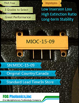
MIOC is a monoblock hermetic product. It includes a linear polarizer, Y-junction coupler and two pairs of electro-optic phase modulators.

LiNbO3 X-cut FOG (Fiber Optic Gyro) chips
LiNbO3 Foundry Services
A foundry service is offered to Customers to exploit the
FOGPHotonics Integrati technological know-how in LiNbO3 processing for
integrated optical circuits.Customer uses the service to get processed wafer,
polished and diced circuits as well as pigtailed and packaged devices.Custom
integrated optical circuits are realised on the basis of the Customer’s designs
or starting from the requirements, exploiting the FOGPhotonics’s design
capabilities.
Product Features
● Annealing Proton Exchange
● High Temperature Proton Exchange (Soft Proton Exchange)
● Fiber pigtailing
● High resolution Poling
● X, Y and Z cuts of LiNbO3,
● Dielectric and metal deposition
● Photolithography
Definition of parameters
The definition of Vπ is the same as the Vπ in
an intensity modulator which interferometric configuration adopts the same
push-pull electrodes (and optical waveguides) used in the gyro chip.
A test amplitude modulator is included
in the wafer. Then we measured the Vπ for this device. The Vπ of an interferometric integrated optical amplitude modulator is
defined as the voltage change requested to move the modulator from the minimum
to the maximum optical transmission. It is a function of frequency f of the
modulating signal V(f), and is defined in the modulator optical transmission
function:

1.1.1 Phase Modulators
The electro-optic effect is used to modulate the optical carrier
fase. In this device a couple of electrodes are located on the sides of a
single waveguide (figure 1) .
The modulator transfer function is simply given by:

Where Δф is the relative phase delay, V is the voltage applied to the electrodes and Vπ is the necessary voltage required to obtain a phase delay equal to π.
1.1.2 Coupling Electrodes
When the
signal is time varying, the simple capacitive electrode configuration, in which
they can be considered a capacitor C in parallel with the terminating resistor
R, is frequency limited by the RC cut. The value of this cut is usually in the
range of 1-2 GHz. In order to obtain modulators efficient enough for the
microwave frequencies (20 GHz), coplanar transmission line configurations are
adopted for the electrodes, allowing Travelling Wave (TW) coupling between the
modulating signal and the optical carrier.
The higher
frequency limit of the TW electrode configuration is possible due to:
the difference
between the propagation speeds of the modulating signal (c/n RF ) and the
optical carrier (c/n opt );
the
resistive/dielectrical losses experimented by the modulating in the coupling
electrodes. The difference
between the propagation speeds is the major limitation to the bandwidth in the
case of conventional TW electrodes. The -3dB bandwidth (BW)is given in this
case by the following expression:

where L is the length of the coupling
between the TW electrodes and the optical waveguide Δn=nRF-nopt is the
difference between the two propagation indexes (typically Δn=2). Because the
efficiency of the modulator (Vπ) decreases with L, wider bandwidths
imply lower electro-optic efficiencies.
Alenia Marconi Systems has developed a
new TW electrode configuration enabling us to overcome this limitation. In this
new configuration, called “Velocity Matched” (VM) the propagation speed of the
modulating signal is adapted to that of the optical carrier. The bandwidth of
the modulator is now limited by resistive/dielectric losses only, which
increase with frequency. Moreover, the electro-optic efficiency is practically
bandwidth independent (figure 2) . This makes the VM increasingly advantageous,
in terms of efficiency, over the conventional TW electrodes as the bandwidth
increases. The electro-optic efficiency of the conventional TW still remains
higher than that of the VM configuration for a bandwidth lower than a threshold
value, typically in the range of 3¸5 GHz. A further advantage of the VM
configuration is the value of the characteristic impedance close to 50 Ohms,
perfectly matched with the external signal line, in spite of the 25-35 Ohms of
the conventional TW electrodes.

Figure 2: Electro-optic efficiency vs bandwidth
Technical Specification
1310nm MIOC Provided by FOGPhotonics
|
Parameter |
Unit |
Values |
| Wavelength |
nm |
1310 |
| Insertion Loss |
dB |
≤4.0 |
| Half wave Voltage |
V |
≤4.0 |
| Splitting Beam Ratio |
- |
47/53-53/47 |
| Optical Return |
dB |
≥50 |
| Polarization extinction ,chip |
dB |
≥55 |
| Additional Intensity Modulating |
- |
≤0.2% |
| PM Pigtail Crosstalk |
dB |
≤-30 |
| Electrode type |
- |
Push-pull modulating |
| Bandwidth |
MHz |
≥300 |
| Pigtail type |
- |
PM |
| Work temperature |
℃ |
-40~+70 |
| Packaging dimensions |
mm |
30X8X5 or 35X10X5 |
| Submount material |
|
Stainless Steel |
| Optical chip length |
mm |
23 |
| Optical chip width |
mm |
2.5 |
| Output Channel Separation |
um |
400 ± 0.2 |
| End-face angle (Z axis) |
deg |
80 ± 0.25 |
| End-face angle (X axis) |
deg |
90 ± 0.25 |
| End-face surface quality |
|
< 3 λ(633 nm) |
1550nm MIOC Provided by FOGPhotonics
| Operation wavelength |
nm |
1550 |
| Vπ(1/2λ differential phase shift) |
v |
4 |
| Insertion loss |
dB |
≤4.0 |
| Intensity modulation |
% |
< 0.1 (+/-Vpi v) |
| Optical Insertion Loss (chip output A+B) (*) |
dB |
2.5 |
| Split Ratio (A/B) |
% |
52/48 |
| Cross Polarisation Rejection (chip) |
dB |
< -55 |
| Cross Polarisation Rejection (Fiber) |
dB |
<-25 |
| Output Channel Separation |
μm |
400 ± 0.2 |
| End-face angle (Z axis) |
deg |
80 ± 0.25 |
| End-face angle (X axis) |
deg |
90 ± 0.25 |
| End-face surface quality |
— |
< 3 λ(633 nm) |
| Bandwidth |
MHz |
300 |
| Maximum Optical input power |
mW |
100 |
| Optical chip length |
mm |
25 |
| Optical chip width |
mm |
2 |
| Operational Temperature |
°C |
-45 - +75 |
| Storage Temperature |
°C |
-40 - +90 |
| Input fiber |
— |
8/125/250 or 6/80/165 Panda |
| Output fibers |
— |
8/125/250 or 6/80/165 Panda |
Applications
● Phase and intensity Electro-Optical modulators
● Multifunctional integrated optical chips for gyros
● High speed polarisation insensitive switches
● PPLN devices

© FOGphotonics, inc. | Company | Products | Technoloy | Contact us


